Our march toward advanced CMOS scaling and new memory technologies has introduced increasingly complex structures to device manufacturing. For instance, in memory an increase in the number of layers to the memory stack in NAND to scale vertically leads to challenges with etching high aspect ratio patterns and more layers to contact in the staircase while preserving the footprint scaling. Unique integration and patterning schemes have been employed to solve the scaling challenges but cause challenges in the design rules.
Two-dimensional (2D) design rule checks (DRCs) are no longer enough to achieve performance and yield goals. Neither is complete reliance on Design of Experiments (DOEs) for process characterization and optimization. Traditionally used to save cost and time in developing recipes, engineers must now resort to hundreds of DOEs that entail significant off-process time and material, including wafers.
Moreover, non-intuitive interactions among process steps, as well as tightening process windows, have made it difficult to deliver concurrent performance and yield optimization using first principle modelling approaches. A 3D understanding of complex process sequences is required and is provided by Coventor SEMulator3D®, a virtual fabrication modelling platform.
What Can SEMulator3D Do?
The software emulates process flows by creating a 3D digital process integration model from a series of unit processing steps. Using a model of the fully integrated process sequence, SEMulator3D can predict the downstream impact of process changes that would otherwise require build-and-test cycles in the fab.
For instance, an engineer can use the software to quickly model a Replacement Metal Gate (RMG) FinFET that uses Trench First Metal Hard Mask (TFMHM) Back End of Line (BEOL) with Self-Aligned Vias (SAV). Once the engineer has confirmed that the 3D representation has been achieved, 2D and 3D metrology and electrical metrics can be extracted.
The software’s electrical analysis module adds resistance and capacitance extraction to help understand process and design sensitivities. This provides a single, and, therefore faster, platform for both 3D modelling as well as validation of electrical function. The process-predictive and silicon accurate structures used in SEMulator3D more precisely reflect fabricated devices than the idealized geometry used in standalone solvers, thereby increasing accuracy.
A DRAM Demonstration
A demonstration of the platform’s ability to model device electric performance based upon variations in etch tool capabilities, such as material selectivity and flux distribution, helps better illustrate the use cases for virtual fabrication. A simple DRAM device case study highlights gate etch behaviour and etch step characteristics required to meet pre-targeted electrical performance and yield.
The demonstration uses the typical workflow for virtual fabrication comprising four steps:
- A nominal process setup that supports process flow calibration and provides a 3D predictive structural representation of the device technology.
- Addition of metrics of interest that qualify the structure or electrical behaviour. These may include metrology, 3D DRCs (design rule checks) and electrical parameters.
- Setup of a design study with DOE (Design of Experiments) and calibration.
- Data analysis, including sensitivity analysis to aid process implementation and/or design change.
Nominal setup
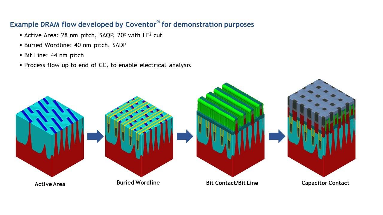
nominal setup for this demonstration is for a 2X DRAM. The process flow was developed by Coventor based upon publicly available data and without using customer confidential information.

The active area (AA) of the DRAM in this demonstration has a 28 nm pitch using self-aligned quadruple patterning (SAQP) and 20°-tilted litho-etch-litho-etch (LELE or LE2) cut. The buried word line has a 40 nm pitch with self-aligned double patterning (SADP) and the bit line has a 44 nm pitch with SADP. The process flow ends at the capacitor contact (CC), which is sufficient to enable electrical analysis in the software and provides the ability to analyse edge effects in the capacitor.
Adding Metrics of Interest
Each process step requires only a few geometric and physical input parameters that are easy to understand and calibrate. The next step in the workflow is to identify those metrics of interest. Just as in an actual fab, unit process parameters, like deposition conformity, etch anisotropy and selectivity, interact with each other and design data in a complex way to impact the final device structure.
SEMulator3D allows the addition of two kinds of geometrical metrology. The first is virtual metrology, which allows the measurement of model structures and verification that features are at their expected dimensions. The second is structure search, which offers steps to examine the entire 3D model or a portion of it to identify measurement extrema, and their values and location for film thicknesses, line widths and contact areas. It also counts the number of material components, which helps to identify electrical net shorts or opens (Figure 2).

The structure search is particularly useful if the location of geometric excursions changes with process variation. For instance, Figure 2 shows the interface area between CC and AA. The software highlights this position, which also happens to be a device fail point.
Electrical Device Simulation
Yet another kind of metric can be extracted using electrical device simulation. Using the same model as shown in Figure 2, the demonstration can proceed to electrical simulation in SEMulator3D.

The software helps identify device ports and electrodes in the 3D structure and simulates the device characteristics, such as temperature, bandgap and electron/hole mobility. It allows for manual as well as automatic identification of nodes (one pin or several tied together), where their initial voltage or current can be set along with voltage sweeps for select nodes.
The electrical simulation example in Figure 3 shows two gates, two sources, one drain and a substrate. Engineers can freely fix the bias or initial voltage as well as the voltage sweep as shown in the DRAM Example Biasing table.
They can then use the software to automatically extract metrics of interest, such as threshold voltage (Vth), sub-threshold slope, drain-induced barrier lowering (DIBL) and ON current (ION) at a voltage point. All of this can be achieved without running time-consuming, rigorous TCAD modelling, while taking into account 3D process effects on electrical performance.
Impact of Geometry Change
A design study into the impact of change in geometry starts with a look at the nominal model that has the hard mask CD/top CD, silicon depth and oxide depth targets established. SEMulator3D has extracted the resulting electrical characteristics using these values, including Vt, ION, IOFF and sub-threshold slope (Figure 4, left).

The objective of this study is to change the hard mask CD in Figure 4 from 12 nm to 30 nm in 2 nm increments, while monitoring the remaining structural parameters, including silicon depth and oxide etch. This change is made by varying the process step early in the flow and the downstream process steps respond predictively to changes in the model.
Figure 4 (right) shows that the hard mask CD change has a non-linear response post gate etch. Oxide depth and top silicon depth are sensitive to top CD at smaller CDs but saturate at larger CDs. On the other hand, Vtsat increases significantly with changing CD above the nominal 20 nm value. Thus, the metrics from SEMulator3D reveal the various responses to a single change in geometry, allowing for engineers to study the impact of geometry change on their chosen parameters.
Identifying Important Process Steps
As a next step, a DOE, consisting of a Monte Carlo variation study, is conducted to identify important process steps (Figure 5). The DRAM Word Line (WL) variation employing Monte Carlo is used in the parameter variation study.

The WL process parameter values are set randomly, based upon Gaussian distribution around a mean or nominal value and standard deviation. In the demonstration, 50 experiments are chosen. However, typically at least a hundred experiments are needed to deliver meaningful research.
The results of the DOE are shown in Figure 6. In the DOE runs, the threshold voltage Vt varies between 0.4837 V and 0.5031 V. The regression analysis by SEMulator3D helps identify five parameters that are significant in terms of the impact they have on the threshold voltage — the p-value of these parameters is less than 0.5, which rejects null hypothesis. Note that the first parameter, intercept, is excluded from this discussion since it is always part of the list.

The five most significant factors identified for further examination are:
- gate dielectric thickness (the most significant parameter),
- cross-term of word line etch and spacer thickness,
- cross-term of mandrel etch depth and gate thickness,
- cross-term of spacer oxide thickness and polish depth, and
- cross-term of gate dielectric thickness and spacer thickness.
The high coefficient of determination (r2) value of 0.97882 in the linear regression plot means that the model fits the data well. The gate oxide thickness versus Vth plot shows strong correlation, whereas the mandrel spacer thickness versus Vth plot does not and can therefore be removed from consideration as a candidate for significant input factors.
The DOE results also help identify corner cases, such as those that are outside the Lower Spec Limit (LSL)-to-Upper Spec Limit (USL) range for Vth, so that engineers can closely examine them and discover the process conditions responsible.
Process Optimization
To take a different perspective on optimization we can instead use the electrical characteristics as the target of the study. This allows the use of electrical targets to be the goal of process step optimization. Each of the process step parameters can be varied to search for a condition that satisfy the electrical performance.
Allowable ranges are defined in software for each etch behaviour depending on the equipment being used. Etch behaviour can thus be defined for such parameters as material etch selectivity, lateral ratios, polymerization/taper, sputtering and ion flux distribution. Using the significant input factors identified by the DOEs, targets are input for electrical performance.
SEMulator3D uses direct optimization to determine the most suitable etch step behavioural process parameters for WL etch such that those electrical targets are satisfied. The calibrated process suggestions include such parameters as oxide, silicon and nitride ratios, oxide and silicon taper, selectivity, and sidewall angle.
With these results, electrical performance can be verified to exist within the process study or that the electrical performance cannot be achieved in that range.
Virtual Processing Saves Cost & Time
Since process assumptions are made during the early stage of development and even before hardware implementation, virtual processing can help validate these assumptions without the time and expense of running real wafers.
This DRAM case study demonstrates that by executing large numbers of DOE and process variation studies in a virtual environment, it is possible to eliminate the time and cost of irrelevant DOE paths and quickly achieve performance and yield goals that will lead to an accelerated time-to-market.
– Joseph Ervin, Director, Semiconductor Process and Integration, Lam Research


